

工业检测量子成像市场(2026—2031)
工业检测量子成像市场预计从2026年的1.622亿美元增至2031年的5.074亿美元,预测期复合年增长率为25.62%;亚太地区既是当前最大市场,也是增长最快的市场。
市场研究正文
规模、增长、细分、驱动因素与关键问题
当前质量分 100.00,审核状态 accepted。结构化字段已按 RoboInd 内容层级组织。
核心结论
工业检测量子成像市场预计从2026年的1.622亿美元增至2031年的5.074亿美元,预测期复合年增长率为25.62%;亚太地区既是当前最大市场,也是增长最快的市场。
市场走势
结构化指标
| 指标 | 年份 | 数值 | 性质 |
|---|---|---|---|
| 复合年增长率 | 2031 | 25.62% | 机构预测 |
| 市场规模 | 2026 | USD 162.2 million | 机构预测 |
| 市场规模 | 2031 | USD 507.4 million | 机构预测 |
细分市场份额
市场结构
| 维度 | 细分项 | 年份 | 份额 |
|---|---|---|---|
| application | Surface Defect Detection | 2025 | 23.450% |
| deployment_mode | Laboratory and Offline Inspection | 2025 | 38.890% |
| end-user_industry | Semiconductor and Electronics | 2025 | 27.760% |
| geography | Asia-Pacific | 2025 | 31.240% |
| quantum_imaging_technology | Quantum Illumination / Quantum-Enhanced Imaging | 2025 | 24.410% |
关键结论
- application 维度中,Surface Defect Detection 在 2025 年的公开份额为 23.45%。
- deployment_mode 维度中,Laboratory and Offline Inspection 在 2025 年的公开份额为 38.89%。
- end-user_industry 维度中,Semiconductor and Electronics 在 2025 年的公开份额为 27.76%。
- geography 维度中,Asia-Pacific 在 2025 年的公开份额为 31.24%。
- quantum_imaging_technology 维度中,Quantum Illumination / Quantum-Enhanced Imaging 在 2025 年的公开份额为 24.41%。
主要参与者
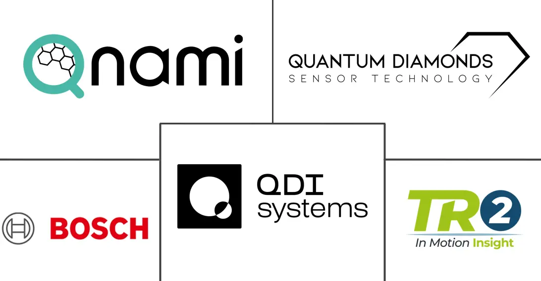
- QuantumDiamonds GmbH
- Qnami AG
- QDI Systems B.V.
- Bosch Quantum Sensing GmbH
- TR2 SRLS
增长驱动因素
| 因素 | 影响 CAGR | 地区相关性 | 影响周期 |
|---|---|---|---|
| Zero-Defect Manufacturing in Advanced Semiconductor Packaging | +6.400% | Global, concentrated in Asia-Pacific, Taiwan, South Korea, and Japan, and North America | Short term (≤ 2 years) |
| Non-Destructive Inspection of Buried and Subsurface Defects | +5.100% | Global, strongest in Asia-Pacific and North America | Medium term (2-4 years) |
| Inline Inspection and Industrial Automation | +4.200% | Asia-Pacific, North America, and Europe | Medium term (2-4 years) |
| Traceability and Functional-Safety Requirements | +3.000% | North America and Europe, with spillover to Asia-Pacific | Medium term (2-4 years) |
| Quantum Advantage in Low-Light and Low-Reflectance Inspection | +2.300% | Global | Long term (≥ 4 years) |
| Commercialization of Room-Temperature Quantum Sensors | +1.800% | Global, with early adoption in Europe and North America | Long term (≥ 4 years) |
市场制约因素
| 因素 | 影响 CAGR | 地区相关性 | 影响周期 |
|---|---|---|---|
| High System Cost and Limited Production-Scale Qualification | -3.700% | Global, most acute outside semiconductor centers in South America and Africa | Medium term (2-4 years) |
| Shortage of Quantum-Optics and Quantum-Metrology Specialists | -1.800% | Global, particularly severe in South America, the Middle East, and Africa | Medium term (2-4 years) |
| Integration Friction With Existing Manufacturing Execution Systems | -1.300% | Global, most pronounced in mature industrial economies with legacy infrastructure | Medium term (2-4 years) |
| Sensitivity to Vibration, Magnetic Interference, and Calibration Conditions | -0.700% | Global, especially relevant for field and at-line deployment | Long term (≥ 4 years) |
报告关注的关键问题
What is the size of the Quantum Imaging for Industrial Inspection Market?
The Quantum Imaging for Industrial Inspection Market is estimated at USD 162.20 million in 2026 and is forecast to reach USD 507.40 million by 2031 at a 25.62% CAGR.
Which technology is growing fastest in quantum imaging for industrial inspection?
Quantum Ghost Imaging is projected to expand at a 26.83% CAGR through 2031, supported by faster SPAD-array image acquisition.
Which application leads the adoption of quantum imaging systems?
Surface Defect Detection held the largest application share at 23.45% in 2025, while Advanced Packaging and Interconnect Inspection is projected to grow fastest.
Why do semiconductor manufacturers use quantum inspection?
The systems support non-destructive detection of difficult defects in advanced nodes, HBM stacks, chiplets, and buried interconnects. For the Quantum Imaging for Industrial Inspection Market, this makes failure analysis an important entry point before systems move into continuous production monitoring.
Which region is leading adoption?
Asia-Pacific held 31.24% share in 2025 and is projected to record a 27.13% CAGR through 2031. The region leads the Quantum Imaging for Industrial Inspection Market because Taiwan, South Korea, Japan, and China have dense semiconductor manufacturing and packaging activity.
What limits wider deployment of quantum inspection equipment?
High system prices, lengthy production qualification, specialist shortages, and factory-integration requirements limit broader near-term deployment. These limits keep the Quantum Imaging for Industrial Inspection Market focused on large semiconductor users, while smaller industrial users remain in earlier evaluation stages.
市场概览
- 增长最快市场:亚太地区
- 最大市场:亚太地区
- 市场集中度:中等
查看来源:Mordor Intelligence