Report Overview
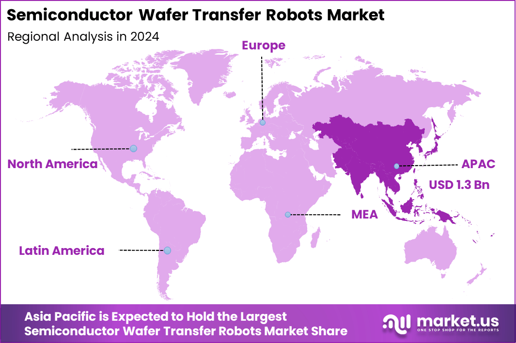
The size of the global Semiconductor Wafer Transfer Robots market reached USD 2.2 billion in 2024 and is anticipated to climb from USD 2.4 billion in 2025 to approximately USD 5.35 billion by 2034, advancing at a CAGR of 9.3% between 2025 and 2034. In 2024, Asia Pacific held a dominan market position, capturing more than a 59.6% share, holding USD 1.3 Billion revenue.
The market for semiconductor wafer transfer robots focuses on robotic and automated systems that handle wafers inside cleanrooms. These robots transfer wafers between process tools, storage cassettes, inspection systems, and measurement stations. They are designed for very high precision and cleanliness because wafers are fragile and sensitive to contamination. Wafer transfer robots are a critical part of fabrication in lithography, etching, deposition, metrology, and test processes.
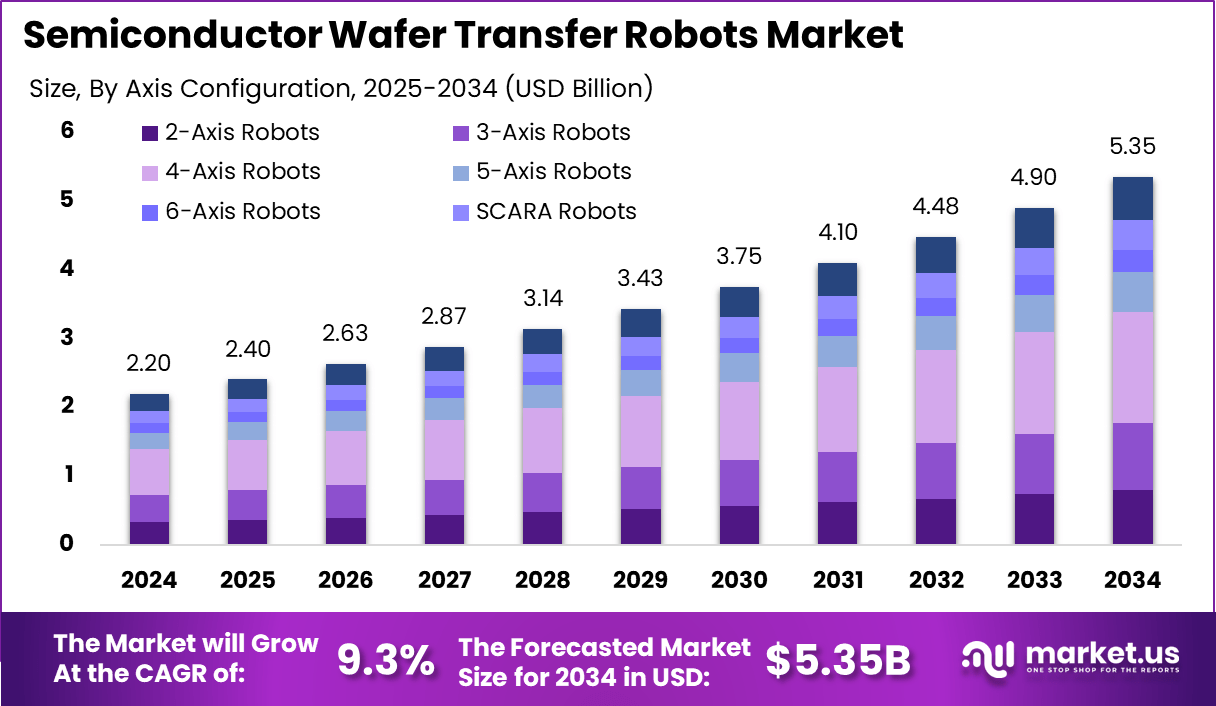
Top driving factors for this market primarily include the rising global demand for electronic devices such as smartphones, 5G infrastructure, automotive electronics, and IoT solutions – all of which require increasingly sophisticated semiconductors. Miniaturization and advanced chips increase the need for robots to handle larger wafers with precision.
According to Market.us, The Global Semiconductor Market was valued at USD 840.6 billion in 2024 and is expected to rise from USD 907.4 billion in 2025 to nearly USD 2,010.6 billion by 2034, expanding at a CAGR of 9.20% during 2025–2034. In 2024, APAC dominated the market with over 65.7% share, generating USD 552.2 billion in revenue.
in parallel, The Analog Semiconductors Market was valued at USD 102.3 billion in 2024 and is forecasted to expand from USD 143.2 billion in 2025 to nearly USD 2,959.1 billion by 2034, at a CAGR of 6.4%. In 2024, Asia-Pacific dominated with more than 45.9% share, accounting for USD 46.9 billion in revenue.
In terms of demand analysis, semiconductor wafer transfer robots see increased adoption due to their ability to minimize contamination risks and human error in fabs. Their automation capabilities reduce operational downtime and accelerate wafer processing cycles, which is critical as fabs scale up production capacities to meet market growth. Government investments and industry efforts drive semiconductor demand growth in Asia-Pacific and North America.
Key Insight Summary
- 4-axis robots hold 30.2%, showing strong adoption for precise wafer transfer tasks.
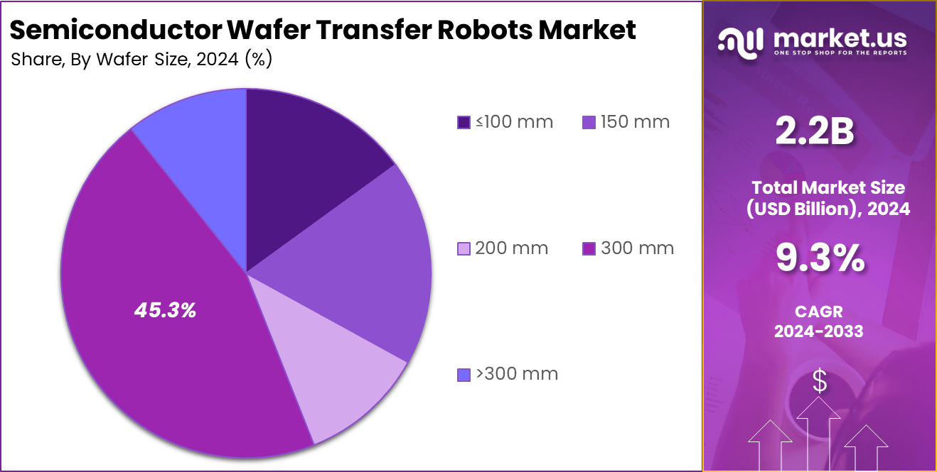
- 300 mm wafer size leads with 45.3%, reflecting the industry’s shift toward larger wafer formats for higher yield.
- Front-end wafer handling accounts for 32.3%, driven by demand in critical chip fabrication processes.
- ISO class 1 cleanroom compatibility represents 40.9%, highlighting strict contamination control in semiconductor manufacturing.
- Integrated robotic systems dominate with 50.5%, as fabs seek higher automation and throughput efficiency.
- Rotary motion robots capture 38.9%, enabling flexibility and speed in wafer transfer operations.
- Foundries lead as end users with 42.5%, supported by large-scale chip production and contract manufacturing growth.
Analysts’ Viewpoint
Technological trends driving adoption include the integration of AI and machine learning for predictive maintenance and real-time quality monitoring, enabling smarter robot operations with reduced downtime. Modular and collaborative robot designs improve flexibility within fabs, while vacuum adsorption and edge-clamping methods enhance wafer handling depending on wafer size and fragility.
The rise of Industry 4.0 principles also encourages deployment of intelligent, connected wafer transfer systems that optimize manufacturing flow. Key reasons for adopting these robots encompass their precision in handling sensitive wafers, reduction of particle contamination through cleanroom compatibility, and the ability to operate continuously with high throughput.
Automated wafer handling supports higher yields by reducing wafer breakage and defects, directly impacting semiconductor fabrication efficiency and quality. Over time, cost savings emerge from less manual intervention, fewer errors, and optimized production cycles despite the initially high investment.
Role of Generative AI
Semiconductor wafer transfer robots are increasingly influenced by generative AI technologies, which are transforming their capabilities beyond simple automation. Generative AI enhances these robots by enabling predictive maintenance that can foresee failures and reduce downtime, leading to more consistent and reliable production processes.
For example, generative AI can analyze complex wafer fabrication workflows to detect inefficiencies and adjust operations on the fly, which helps manufacturers meet growing demand for precision and speed in semiconductor production. Studies show that adoption of AI in wafer transfer robotics has improved operational uptime by over 15%, marking a significant step forward in efficiency.
Investment and Business Benefits
Investment opportunities exist in expanding wafer robot technologies aligned with emerging semiconductor manufacturing trends, such as adapting robots for larger wafer sizes (e.g., 450mm) and incorporating environmentally sustainable, energy-efficient designs.
Increasing automation within fabs driven by 5G, AI, and IoT growth fuels demand for advanced wafer transfer systems, creating room for innovation and partnerships focused on smart fabs. Emerging markets in Asia-Pacific offer particularly fertile ground for investments as semiconductor fabrication capabilities expand rapidly.
The business benefits of semiconductor wafer transfer robots include enhanced accuracy and operational consistency, minimized contamination, lower production costs over time, and increased facility throughput. These robots facilitate leaner manufacturing processes and support complex chip production requirements, thus giving fabs a competitive edge in quality and speed. Additionally, reliance on automated systems reduces labor intensity and contributes toward safer, controlled manufacturing environments.
By Axis Configuration
In 2024, the 4-axis robots segment held 30.2% of the semiconductor wafer transfer robots market. These robots are widely used because they combine high precision with simpler mechanics, making them effective in repetitive wafer transfer operations. Their cost-effectiveness and ability to achieve reliable placement accuracy make them a preferred choice in fabs handling medium to high throughput requirements.
In semiconductor manufacturing, precision is non-negotiable, and 4-axis robots fit well into production lines where efficiency and stability take priority. They are designed to handle delicate wafers without compromising speed, which helps in maintaining a steady throughput across fabrication facilities.
By Wafer Size
In 2024, The 300 mm wafer size dominated with 45.3% share. Larger wafer sizes are adopted to maximize output per wafer and reduce overall manufacturing costs, making 300 mm a standard in advanced semiconductor production. Transfer robots supporting this size are engineered to manage the increased wafer weight while minimizing vibration and particle contamination.
With the shift toward finer geometries and higher device integration, 300 mm wafer handling has become central to modern fabs. Robots in this category help eliminate human error during wafer loading and unloading, which ensures higher yield rates in critical process steps.
By Application
In 2024, Wafer handling in front-end process accounted for 32.3% of demand. This stage involves critical steps like lithography, cleaning, and deposition, where careful handling ensures minimal defects. Transfer robots here play a key role in keeping wafers free of microcontamination and physical stress.
As front-end processes are highly sensitive, automation using these robots reduces risks associated with manual intervention. The use of robots helps maintain the uniformity and reliability needed to achieve consistent semiconductor device performance.
By Cleanroom Compatibility
In 2024, The ISO Class 1 cleanroom compatible robots segment represented 40.9% of the market. These robots are designed for environments with the strictest contamination control, which is required for advanced semiconductor fabrication. Their construction minimizes particle generation and supports sterile wafer transfers.
As chip designs become more complex, wafers are more prone to damage from even microscopic contaminants. Robots capable of functioning in ISO Class 1 environments ensure that processes remain consistent and reliable, protecting overall yield.
By Level of Automation
In 2024, Integrated robotic systems captured 50.5% market share. These systems combine multiple handling tasks with seamless process integration, reducing time and cost while improving throughput. Their ability to link wafer handling with tools such as inspection and cleaning modules makes them highly efficient.
The growing use of integrated systems reflects the industry’s need to build fully automated fabs. By reducing dependency on standalone robots, integrated systems streamline operations and enable fabs to meet the demand for higher productivity and tighter process control.
By Motion Type
In 2024, Rotary motion robots accounted for 38.9% of the market. They are valued for their ability to transfer wafers smoothly while optimizing space in constrained cleanroom layouts. Their design allows higher maneuverability, which supports the precise demands of wafer positioning during transfer.
The increasing use of rotary configurations comes from their adaptability to both standard and complex process workflows. Their efficiency helps improve throughput while ensuring wafer integrity, an advantage for fabs aiming to scale production.
By End User
In 2024, Foundries contributed 42.5% market share. As contract manufacturers for a wide range of semiconductor devices, foundries rely heavily on wafer transfer robots to handle high-volume production at varying process nodes. Automation here directly supports yield improvement and cycle time reduction.
Since foundries operate with a diverse customer base, flexibility is crucial. Robots allow foundries to handle different wafer sizes and processes with minimal reconfiguration, aligning perfectly with the dynamic nature of the business.
Emerging Trends
Emerging trends in the semiconductor wafer transfer robots market include greater integration with Industry 4.0 frameworks, modular robot designs for flexibility, and energy-efficient technologies that reduce power consumption without sacrificing performance. There is a noticeable shift toward robots that can handle larger wafers, such as 300mm and even 450mm sizes, which offer cost advantages and higher throughput.
These robots increasingly feature real-time monitoring systems and diagnostics to predict maintenance needs before breakdowns occur. The market is also moving toward enhanced precision engineering with better sensors and control systems, delivering improved handling accuracy critical for advanced semiconductor fabrication processes. These trends reflect a growing demand for precision, adaptability, and sustainability in manufacturing environments.
Growth Factors
Growth factors driving the semiconductor wafer transfer robot market stem from the rising global demand for semiconductors, fueled by strong growth in electronics, 5G infrastructure, artificial intelligence, and IoT devices. The drive for miniaturization in electronic components intensifies the need for robots that can manage delicate and precise wafer transfers within cleanroom environments.
Furthermore, the demand for high-performance chips used in areas like AI and high bandwidth memory significantly contributes to the need for advanced wafer handling robots. Data indicates the market has experienced a compound annual growth rate exceeding 8% recently, attributed largely to these expanding applications and production demands.
Key Market Segments
By Axis Configuration
- 2-Axis Robots
- 3-Axis Robots
- 4-Axis Robots
- 5-Axis Robots
- 6-Axis Robots
- SCARA Robots
- Cartesian Robots
By Wafer Size
- ≤100 mm
- 150 mm
- 200 mm
- 300 mm
- >300 mm
By Application
- Wafer Handling in Front-End Process
- Back-End Packaging & Assembly
- Metrology & Inspection
- Cleaning & Etching
- Lithography
- Ion Implantation
- Deposition (PVD, CVD, ALD)
- CMP (Chemical Mechanical Planarization)
By Cleanroom Compatibility
- ISO Class 1
- ISO Class 2
- ISO Class 3
- ISO Class 4 and above
By Level of Automation
- Standalone Robotic Arms
- Integrated Robotic Systems
- AMR (Autonomous Mobile Robots) with Wafer Transfer Modules
By Motion Type
- Linear Motion Robots
- Rotary Motion Robots
- Hybrid Motion Robots
By End User
- IDM (Integrated Device Manufacturers)
- Foundries
- OSAT (Outsourced Semiconductor Assembly and Test)
- Research & Academic Institutions
- Equipment OEMs
Regional Insight
In 2024, APAC held a dominant market position, capturing more than 59.6% share and generating USD 1.3 billion in revenue in the semiconductor wafer transfer robots market. The region’s leadership is primarily driven by its strong semiconductor manufacturing base, with countries such as Taiwan, South Korea, China, and Japan accounting for the majority of global chip production.
The high concentration of fabrication plants and assembly facilities in APAC has fueled large-scale adoption of wafer transfer robots to improve precision, reduce contamination, and increase production efficiency in cleanroom environments. APAC’s dominance is further supported by rising investments in advanced semiconductor technologies, particularly in logic and memory chips that require ultra-clean and automated handling processes.
Governments in the region are actively supporting the expansion of local semiconductor industries through subsidies and policy incentives, which in turn accelerate the deployment of automation solutions. Moreover, the presence of leading global equipment manufacturers and regional suppliers has created an ecosystem that enables faster adoption of wafer handling robotics at competitive costs.
Regional Analysis and Coverage
- North America
- US
- Canada
- Europe
- Germany
- France
- The UK
- Spain
- Italy
- Russia
- Netherlands
- Rest of Europe
- Asia Pacific
- China
- Japan
- South Korea
- India
- Australia
- Singapore
- Thailand
- Vietnam
- Rest of Latin America
- Latin America
- Brazil
- Mexico
- Rest of Latin America
- Middle East & Africa
- South Africa
- Saudi Arabia
- UAE
- Rest of MEA
Driver Analysis
Rising Demand for Semiconductors in Consumer Electronics
The rising demand for consumer electronics is driving the growth of the semiconductor wafer transfer robots market. With the increasing adoption of smartphones, laptops, IoT devices, and AI-enabled systems, the need for semiconductors is growing rapidly. To meet this demand, manufacturers are focusing on improving production efficiency, speed, and precision.
Wafer transfer robots support this goal by automating wafer handling in cleanroom environments, ensuring accuracy and higher throughput. For instance, the U.S. consumer electronics market is expected to reach $505 billion in 2024, reflecting strong and steady demand that directly benefits wafer transfer automation adoption.
These robots reduce contamination risks and improve productivity by precisely moving delicate wafers through complex manufacturing stages. The push for advanced semiconductor types such as high-performance chips in AI, 5G, and other technologies furthers this trend. Thus, the wafer robot market grows alongside the expanding semiconductor fabrication sector, driven by ongoing innovation and demand for smaller, faster electronic devices.
Restraint Analysis
High Initial and Maintenance Costs
One major restraint facing the semiconductor wafer transfer robots market is the high cost associated with purchasing, installing, and maintaining these advanced robotic systems. The initial investment can be prohibitive, especially for small and medium-sized manufacturers, which may find it hard to justify the expense in competitive environments.
Moreover, these robots require frequent upkeep, calibration, and occasional repairs to maintain their precision and reliability, which adds ongoing operational costs. For instance, advanced wafer transfer robots can cost between USD 250,000 to USD 600,000 per unit, with annual maintenance costs reaching 10-15% of the equipment’s value. These financial hurdles slow adoption rates among smaller fabs and labs, as does the need for skilled operators who command higher labor costs.
Opportunity Analysis
Expansion Driven by 5G and Emerging Technologies
The growth of emerging technologies such as 5G, artificial intelligence, and electric vehicles presents a significant opportunity for semiconductor wafer transfer robots. These technologies require increasingly sophisticated and high-performance chips, boosting semiconductor production volumes and the complexity of manufacturing processes.
As chip designs grow more advanced, precise wafer handling becomes critical to ensure quality and yield, opening new business avenues for wafer transfer robot manufacturers. The transition to larger wafer sizes, such as 450mm wafers, also creates demand for robots capable of handling heavier and larger wafers with high accuracy.
Additionally, governments and investors worldwide are targeting semiconductor production capacity expansion, adding to demand for automation technology. These factors collectively create a promising environment for wider adoption of wafer transfer automation in the coming years.
Challenge Analysis
Integration and Interoperability Complexities
A notable challenge for the semiconductor wafer transfer robots market is the complexity involved in integrating these robotic systems with existing manufacturing infrastructure. Semiconductor fabrication facilities operate with highly specialized and sometimes legacy equipment, making seamless integration of new robots difficult.
Differences in interfaces, communication protocols, or software standards often cause compatibility issues. For example, retrofitting older production lines with wafer transfer robots requires costly adjustments and can lead to production delays.
Moreover, the technology evolves rapidly, causing companies to hesitate in investing due to risks of obsolescence. Skilled personnel are needed to manage this complexity, but labor shortages hinder smooth implementation. These factors slow down adoption and complicate scaling automation efforts in semiconductor fabs.
Competitive Analysis
The Semiconductor Wafer Transfer Robots Market is supported by global automation leaders such as KUKA AG, Yaskawa Electric Corporation, Kawasaki Robotics, and Yamaha Robotics. These companies provide advanced robotic systems designed for high precision, speed, and reliability in semiconductor fabs.
Specialized players including Hirata Corporation, JEL Corporation, Shibaura Machine, Brooks Automation, and Rorze Corporation dominate in wafer transfer solutions tailored for cleanroom environments. These firms focus on robotic arms, end-effectors, and automation modules that enable safe transfer of delicate wafers across lithography, etching, and deposition stages.
Emerging and regional players such as Siasun Robot & Automation Co., TAEHA Mechatronics, HIWIN Technologies, Nidec Sankyo Corporation, Robostar Co., Ltd., and Tazmo Co., Ltd. are expanding their market presence with cost-effective and flexible wafer handling systems. Companies like DAIHEN Corporation, RAONTEC Inc., Kensington Laboratories, and AUTOMATECH Robotics also contribute through customized robotic solutions.
Top Key Players in the Market
- KUKA AG
- Hirata Corporation
- JEL Corporation
- Yamaha Robotics
- Shibaura Machine (formerly Toshiba Machine)
- Kensington Laboratories
- Siasun Robot & Automation Co.
- TAEHA Mechatronics
- HIWIN Technologies Corp.
- Nidec Sankyo Corporation
- Brooks Automation
- Yaskawa Electric Corporation
- Rorze Corporation
- Kawasaki Robotics
- Robostar Co., Ltd.
- DAIHEN Corporation
- RAONTEC Inc.
- AUTOMATECH Robotics
- HIRATA FA Engineering
- Tazmo Co., Ltd.
- Others
Recent Developments
- September 2025 – JEL Corporation: JEL participated in SEMICON Korea 2024 highlighting its lead in cleanroom wafer handling robots designed for semiconductor and FPD substrate transfer. JEL continues to strengthen its product showcase and market presence in Asia.
- October 2024 – Siasun Robot & Automation: Siasun expanded its global footprint with mobile robots enhancing battery handling and logistics for new energy companies. Its semiconductor and robotics divisions reported a 10.37% revenue increase year-on-year, indicating robust growth.