Report Overview
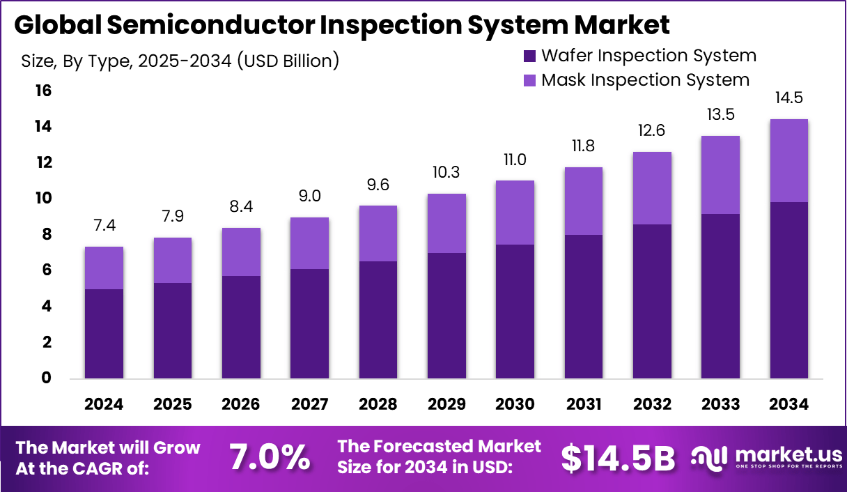
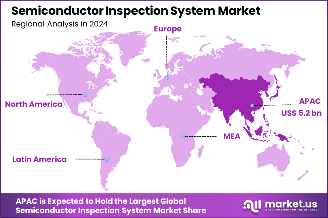
The Global Semiconductor Inspection System Market size is expected to be worth around USD 14.5 Billion By 2034, from USD 7.4 billion in 2024, growing at a CAGR of 7.0% during the forecast period from 2025 to 2034. In 2024, APAC held a dominant market position, capturing more than a 71.0% share, holding USD 5.2 Billion revenue.
Semiconductor inspection systems employ a range of sophisticated technologies, such as optical microscopy, laser scattering, and electron beam inspection, to meticulously identify and evaluate defects, scratches, and contaminations on wafers and packaged devices. This critical scrutiny is essential for maintaining stringent quality control throughout the manufacturing process.
The global market for Semiconductor Inspection Systems is experiencing robust growth, driven by the increasing demand for high-quality semiconductor devices. The market’s expansion can be attributed to advancements in technology and the scaling production demands of industries like consumer electronics and automotive.
The demand for advanced semiconductor components is rising due to the proliferation of technologies such as smartphones, 5G, artificial intelligence (AI), and Internet of Things (IoT) devices. This demand necessitates highly reliable semiconductor components, thus fueling the need for sophisticated inspection systems capable of detecting minute defects that could impact device performance and reliability.
There is a significant push towards the miniaturization of semiconductor devices, leading to a greater need for advanced inspection systems. These systems must possess high resolution and sensitivity to effectively manage the intricacies of smaller semiconductor structures. Additionally, the trend towards automated manufacturing in the semiconductor industry is increasing the integration of inspection systems into production lines to provide real-time quality control.
As reported by Market.us, The global semiconductor market is projected to expand significantly, with its valuation expected to reach approximately USD 996 billion by 2033, up from USD 530 billion in 2023. This growth represents a CAGR of 6.5% over the forecast period from 2024 to 2033. In 2023, the Asia-Pacific (APAC) region maintained a dominant stance in the market, securing more than a 63.91% share, which equated to USD 388.7 billion in revenue.
The semiconductor industry is rapidly adopting new inspection technologies that offer enhanced capabilities such as high throughput, greater sensitivity, and the ability to handle complex chip architectures like 3D stacking and advanced packaging. These advancements are crucial for maintaining the pace with the miniaturization and complexity of modern semiconductor devices.
Key Takeaways
- The Global Semiconductor Inspection System Market is poised for steady growth over the next decade. It is expected to reach a value of around USD 14.5 billion by 2034, increasing from USD 7.4 billion in 2024. This growth represents a CAGR of 7.0% during the forecast period from 2025 to 2034.
- Asia-Pacific continues to dominate the market. In 2024, the region accounted for over 71.0% of the global market share, generating approximately USD 5.2 billion in revenue.
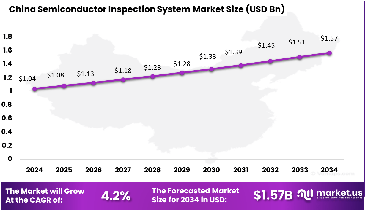
- The China Semiconductor Inspection System Market was valued at approximately USD 1.04 billion in 2024 and is forecast to grow to USD 1.57 billion by 2034, at a projected CAGR of 4.2% from 2025 onward.
- When analyzing by type, Wafer Inspection Systems emerge as the most dominant segment, accounting for nearly 68% of the market share.
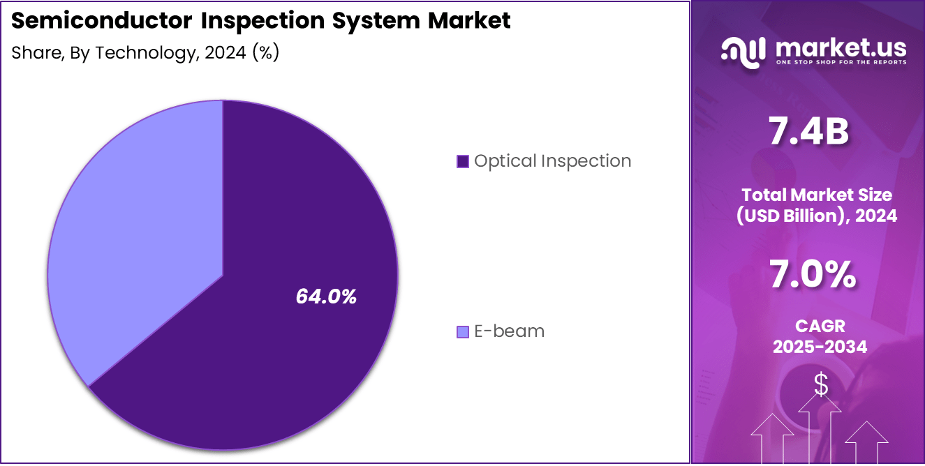
- By technology, Optical Inspection remains the leading approach, holding a share of approximately 64%. Optical methods are favored due to their high-speed capabilities and non-invasive nature, which are essential for early-stage fault detection and quality assurance.
- In terms of end-user segments, Foundries represent the largest share, contributing around 40% of the total market.
Analysts’ Viewpoint
The expansion of semiconductor manufacturing in emerging markets presents significant investment opportunities for providers of inspection systems. Additionally, the ongoing advancement in packaging techniques and the integration of AI and machine learning in inspection processes highlight areas where investment can lead to substantial business benefits, such as improved yield rates and production efficiencies.
Recent technological advancements in inspection systems include the development of high-power, ultra-uniform illumination systems, and AI-driven image processing that enhances the detection capabilities of inspection tools. These innovations not only improve the accuracy but also the speed of inspections, making them more efficient and reducing the overall production costs.
The semiconductor industry is highly regulated to ensure the reliability and safety of electronic devices. Inspection systems play a vital role in complying with these regulations by ensuring that every component meets the required standards before it is integrated into larger systems or devices.
Impact of AI
- Enhanced Defect Detection and Classification: AI significantly improves the ability of semiconductor inspection systems to detect and classify defects. By leveraging machine learning algorithms, these systems can accurately identify defects that traditional methods might miss, thereby reducing false positives and improving the quality of semiconductor devices.
- Real-Time Processing and Feedback: AI integration allows for the real-time analysis of data during the semiconductor manufacturing process. This capability enables immediate corrections and adjustments, minimizing the propagation of errors and reducing potential yield loss. Such systems can analyze vast amounts of inspection data quickly, aiding in faster decision-making.
- Increased Throughput and Efficiency: AI-driven semiconductor inspection systems can operate at higher speeds compared to traditional systems, thus increasing the throughput. By automating the inspection process, AI reduces the time needed for manual inspections and speeds up the overall manufacturing process.
- Cost Reduction and Yield Improvement: The application of AI in semiconductor inspection can lead to significant cost savings and yield improvements. AI systems optimize the inspection process, detect defects early, and reduce the wastage of materials, contributing to overall operational efficiency and lower production costs.
- Adaptability and Continuous Learning: AI systems in semiconductor inspection are adaptable and capable of continuous learning. They can improve over time based on new data, adjusting to changes in manufacturing processes or new types of semiconductor devices. This adaptability ensures that the inspection systems remain effective as technology evolves and as new challenges in semiconductor manufacturing arise.
China Market Growth
The China Semiconductor Inspection System Market is valued at approximately USD 1.04 Billion in 2024 and is predicted to increase from USD 1.08 Billion in 2025 to approximately USD 1.57 Billion by 2034, projected at a CAGR of 4.2% from 2025 to 2034.
In 2024, the Asia-Pacific (APAC) region held a dominant position in the semiconductor inspection system market, capturing more than a 71% share. This substantial market share translated to revenues exceeding USD 5.2 billion. The prominence of APAC in this sector can be attributed to several key factors.
Firstly, the region hosts a significant concentration of semiconductor manufacturing facilities, particularly in countries such as South Korea, Taiwan, and China. These countries are home to some of the world’s largest semiconductor companies, which demand advanced inspection systems to enhance the reliability and performance of their semiconductor devices.
Furthermore, the rapid growth of the electronics industry in APAC has driven the demand for semiconductor inspection systems. The increasing consumer electronics production, coupled with the expansion of telecommunication networks in the region, has necessitated the deployment of more sophisticated inspection technologies to maintain high-quality standards in semiconductor manufacturing.
Advancements and Applications
The semiconductor inspection system market is crucially supported by a variety of sophisticated techniques and technologies aimed at enhancing the quality and efficiency of semiconductor manufacturing. Here’s a detailed overview of the primary methods and applications:
Techniques and Technologies
- Optical Microscopy: Utilizes different lighting and contrast techniques, including brightfield, darkfield, polarization, Differential Interference Contrast (DIC), ultraviolet (UV), oblique illumination, and infrared (IR). This method supports a range of magnifications to facilitate effective visual inspection.
- Laser Scattering: Involves scanning a laser beam across the wafer surface. The detection of scattered light from this process helps identify surface defects and particulate contaminants.
- Electron Beam Inspection: Employs an electron beam to scan the wafer surface. The detection of secondary and backscattered electrons emitted provides detailed insights into surface defects and material contrasts.
- AI and Machine Learning: These technologies are increasingly integrated to analyze inspection data, enhance the accuracy of defect detection, and minimize the occurrence of false positives.
Applications
- Wafer Inspection: Critical for detecting particles, scratches, and other defects on wafers both before and after the patterning process.
- Package Inspection: Focuses on examining packaged devices to identify defects in wire bonds, solder joints, and overall package integrity.
- Advanced Packaging Inspection: Involves the inspection of cutting-edge packaging technologies, including 3D integrated circuits (ICs) and chip-on-wafer (COW).
- Defect Analysis and Classification: Aims at determining the root causes of defects and categorizing them to inform process improvements.
Key Benefits
- Improved Quality Control: Ensures the production of high-quality semiconductors.
- Increased Yield: By reducing the incidence of defects, inspection systems contribute to higher production yields.
- Faster Time to Market: Facilitates quicker identification and resolution of manufacturing issues, accelerating product development.
- Reduced Manufacturing Costs: Effective inspection systems help prevent defects and boost yield, thereby lowering overall manufacturing expenses.
Examples of Semiconductor Inspection Systems
- Wafer Surface Inspection System LS Series (Hitachi High-Tech): Employs laser scattering technology to detect defects on unpatterned wafers with a mirror-finished surface.
- Dark Field Wafer Defect Inspection System DI2800 (Hitachi High-Tech): Uses scattering-intensity simulation technology for highly sensitive inspection of defects on patterned wafers.
- Wafer Chip Inspection System Model 7940 (Chroma ATE Inc.): Features a user-friendly interface for efficient wafer mapping and defect analysis.
- Semiprobe Wafer Inspection System (WIS): Designed to examine, locate, and identify defects occurring during wafer manufacturing.
- Applied Materials Metrology and Inspection Systems: Provides a comprehensive suite of metrology, inspection, and review systems for front-end of line (FEOL) and back-end of line (BEOL) applications.
- Hamamatsu Photonics Wafer Inspection Systems: Utilizes high-precision electron beam detection for wafer inspection.
Type Analysis
In 2024, the Wafer Inspection System segment held a dominant market position in the semiconductor metrology and inspection sector, capturing more than a 68% share. This leadership can be attributed to several compelling factors that underscore the segment’s critical role in modern semiconductor manufacturing.
The need for highly precise inspection systems has escalated with the advent of sophisticated semiconductor designs and the integration of more complex technologies. Wafer inspection systems are essential for identifying defects and verifying the quality of wafers during the semiconductor manufacturing process. As devices become smaller and circuits more densely packed, the precision these systems provide becomes crucial for maintaining high yield rates and operational efficiency.
A significant driver of the Wafer Inspection System’s market dominance is the increasing demand for three-dimensional integrated circuits, commonly used in devices ranging from smartphones to advanced computing systems. This demand has spurred the need for inspection technologies that can accommodate the intricate architecture of these components.
Additionally, the surge in the adoption of 300mm wafers, particularly in LED applications and for efficient temperature control in thin wafers, has further propelled the growth of this market segment. The incorporation of artificial intelligence (AI) and machine learning (ML) into wafer inspection systems has revolutionized their capabilities, enabling faster throughput and more precise defect detection.
Technology Analysis
In 2024, the Optical Inspection segment maintained a dominant market position within the semiconductor inspection system industry, capturing more than a 64% share. This significant market share is attributed to several key factors that highlight the indispensability and effectiveness of optical inspection technologies in semiconductor manufacturing.
Optical inspection systems are highly valued for their ability to quickly and efficiently detect a wide range of defects across semiconductor wafers. This capability is crucial given the increasing complexity of semiconductor designs and the constant push for miniaturization in the industry. The systems utilize advanced imaging techniques to ensure high-quality production and adherence to stringent manufacturing standards.
The field has seen substantial innovations, such as the integration of AI and machine learning, which enhance the capabilities of optical inspection systems. These technologies allow for better anomaly detection and process optimization by analyzing data collected during the inspection process. This adaptation has made optical inspection systems even more critical as they evolve to meet the demands of modern semiconductor manufacturing processes.
The growing demand for consumer electronics, telecommunications, and automotive technologies continues to drive the need for reliable semiconductor components. Optical inspection systems play a pivotal role in ensuring the production of high-quality wafers needed to support these technologies, thus underpinning the segment’s market dominance. The broad applicability of optical inspection across various manufacturing stages – from wafer fabrication to final quality assurance – further solidifies its market position.
End-User Analysis
In 2024, the Foundries segment held a dominant market position in the semiconductor inspection system industry, capturing more than a 40% share. This leading role is underscored by several key factors that are pivotal to the segment’s market influence and its critical function within the semiconductor production landscape.
Foundries are at the heart of semiconductor manufacturing, providing essential fabrication services that span a wide range of applications, from consumer electronics to industrial components. This central role ensures a steady demand for precise and effective inspection systems to maintain high quality and yield standards, which are critical for the reliability of the end products.
The segment’s dominance is further reinforced by continuous technological advancements and substantial investments in metrology and inspection equipment. Foundries are often at the forefront of adopting cutting-edge technologies to enhance their manufacturing processes, ensuring the detection of even the minutest defects that could affect semiconductor performance.
As semiconductor devices become more complex, the role of foundries in maintaining manufacturing precision becomes even more critical. Advanced inspection systems are utilized to handle the challenges of shrinking transistor sizes and 3D integration, which are prevalent in modern semiconductor designs. This capability to manage and inspect intricate designs effectively supports their leading position in the market.
Key Market Segments
By Type
- Wafer Inspection System
- Mask Inspection System
By Technology
- Optical Inspection
- E-beam
By End-User
- IDMs (Integrated Device Manufacturers)
- OSATs
- Foundries
- Memory Manufacturers
Driver
Integration of Artificial Intelligence and Machine Learning
The integration of Artificial Intelligence (AI) and Machine Learning (ML) in semiconductor inspection systems is a significant driver of the market. These technologies enhance the accuracy and efficiency of inspection processes by enabling faster and more precise defect detection. AI algorithms analyze data collected during inspections to identify patterns and anomalies that might indicate potential failures or defects.
This capability is crucial in modern semiconductor manufacturing where the complexity and miniaturization of devices demand high precision and reliability. The adoption of AI and ML not only improves the detection capabilities but also reduces the time required for inspections, thereby increasing throughput and reducing costs. As semiconductor devices become more complex, the role of AI in ensuring quality and consistency in production becomes increasingly vital.
Restraint
High Cost of Advanced Inspection Systems
A major restraint in the semiconductor inspection system market is the high cost associated with advanced inspection technologies. The development, procurement, and maintenance of sophisticated inspection systems require substantial investment.
For smaller manufacturers or startups, these costs can be prohibitive, limiting their ability to compete with larger entities that can more easily afford such advanced technologies. The need for continual upgrades to keep pace with rapidly advancing semiconductor technologies further escalates costs, posing a significant barrier to entry and expansion for smaller players in the industry.
Opportunity
Expansion of Semiconductor Manufacturing in Emerging Markets
Emerging markets present significant opportunities for the expansion of the semiconductor inspection system industry. Countries like China and India are rapidly developing their semiconductor manufacturing capabilities, fueled by government initiatives and growing local demand for electronic devices.
This expansion is driving the demand for high-quality inspection systems to ensure the reliability and performance of produced semiconductors. Manufacturers of inspection systems can tap into these new markets, expanding their global footprint and driving growth by meeting the increasing needs for semiconductor inspection in these regions.
Challenge
Rapid Technological Changes and Skilled Labor Shortage
One of the primary challenges in the semiconductor inspection system market is the rapid pace of technological changes. Inspection systems must continually evolve to address the latest developments in semiconductor manufacturing, such as new materials, 3D ICs, and complex circuit designs. This rapid evolution requires ongoing research and development, which is resource-intensive.
Additionally, there is a significant challenge in sourcing skilled labor capable of developing, operating, and maintaining these advanced systems. The complexity of modern semiconductor inspection technologies demands a highly skilled workforce, and the shortage of such talent can impede the growth and innovation in the industry.
Growth Factors
- Increasing Demand for Advanced Semiconductors: The global market for semiconductor inspection systems is significantly driven by the growing need for high-quality, advanced semiconductor devices. This demand is propelled by the widespread adoption of smartphones, 5G technology, AI, and IoT devices. These technologies require highly reliable semiconductor components, thus necessitating robust inspection systems to ensure their quality and performance.
- Miniaturization of Semiconductor Devices: As semiconductor devices continue to shrink in size, the complexity of inspecting these tiny components increases. This trend towards miniaturization requires more sophisticated, high-resolution, and high-sensitivity inspection systems capable of detecting extremely small defects that could potentially affect device performance.
- Integration of Advanced Technologies: The integration of cutting-edge technologies, such as AI and machine learning, into semiconductor inspection systems enhances their capability to identify defects accurately and efficiently. This integration supports the handling of complex data and improves the systems’ overall efficiency and effectiveness in spotting critical issues.
Emerging Trends
- Technological Advancements: Recent advancements in semiconductor inspection technologies include the development of systems equipped with higher resolution imaging and advanced analytical capabilities. These improvements are crucial in managing the increasing complexity of semiconductor device architectures, such as 3D integration and advanced packaging, which require meticulous inspection to ensure device reliability and performance.
- Globalization of Semiconductor Manufacturing: The semiconductor manufacturing landscape is becoming increasingly globalized, with significant growth opportunities emerging in Asia-Pacific, Latin America, and other regions. This expansion is fostering a heightened demand for semiconductor inspection systems that can support the scaling production needs of these diverse markets.
Business Benefits
- Enhanced Quality Control: Modern semiconductor inspection systems equipped with AI and machine learning offer superior quality control by enabling more precise defect detection. This precision helps in reducing the wastage of materials and ensures that only the highest quality products proceed to the next stages of manufacturing.
- Increased Manufacturing Efficiency: By automating the inspection process and integrating systems directly into the production lines, these advanced systems minimize the downtime that typically comes with manual inspections. This integration significantly boosts the throughput and efficiency of semiconductor manufacturing processes.
- Cost Reduction: Advanced inspection systems can detect defects early in the manufacturing process, reducing the cost associated with defective products reaching later stages of production. Early detection helps in minimizing scrap rates and enhances the overall yield, which in turn, reduces the production costs.
Key Regions and Countries
- North America
- US
- Canada
- Europe
- Germany
- France
- The UK
- Spain
- Italy
- Rest of Europe
- Asia Pacific
- China
- Japan
- South Korea
- India
- Australia
- Singapore
- Rest of Asia Pacific
- Latin America
- Brazil
- Mexico
- Rest of Latin America
- Middle East & Africa
- South Africa
- Saudi Arabia
- UAE
- Rest of MEA
Key Player Analysis
KLA Corporation has solidified its position in the semiconductor inspection system market through strategic acquisitions and innovative product launches. The company’s commitment to expanding its technological capabilities can be seen in its recent acquisitions, which enhance its product lineup and market reach.
Applied Materials is renowned for its comprehensive portfolio of semiconductor solutions, including advanced inspection systems. The company’s strategy often involves merging with relevant tech enterprises to broaden its technological expertise and market footprint.
ASML Holding is a leading player in the semiconductor industry, particularly known for its photolithography systems essential for semiconductor manufacturing. The company also excels in developing sophisticated inspection systems that complement its main offerings.
Top Key Players in the Market
- KLA Corporation
- Applied Materials
- ASML Holding
- Hitachi High-Tech
- Onto Innovation
- NanoPhotonics
- Lasertech
- JEOL Ltd.
- Herms Microvision
- Lam Research
- FEI
- Carl Zeiss
- Nikon
- Planar Corporation
- Rudolph Technologies
- Other Key Players
Recent Developments
- October 2024: KLA Corporation introduced a comprehensive portfolio of process control and enabling solutions for integrated circuit (IC) substrate manufacturing. This initiative aims to assist customers in achieving breakthroughs in packaging interconnect density for high-performance applications.
- March 2024: Hitachi High-Tech introduced the LS9300AD, a semiconductor inspection system equipped with a new Differential Interference Contrast (DIC) optical system. This innovation enables high-sensitivity and high-throughput inspection, facilitating the detection of low-aspect microscopic defects.
- April 2024: Onto Innovation released a sub-surface defect inspection capability for its Dragonfly® G3 system. This enhancement allows comprehensive wafer inspection for critical sub-surface defects, addressing the needs of advanced packaging applications.